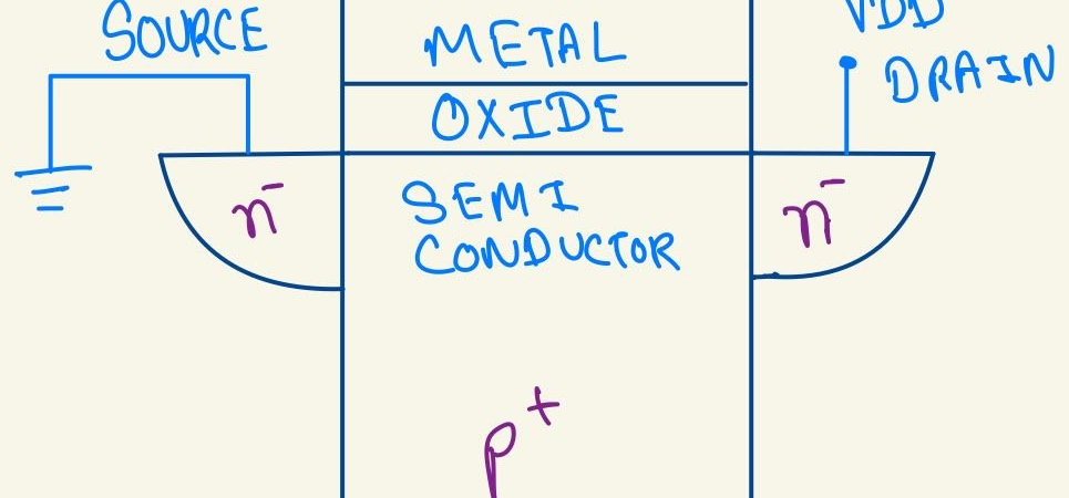
MOSFET Diagram:
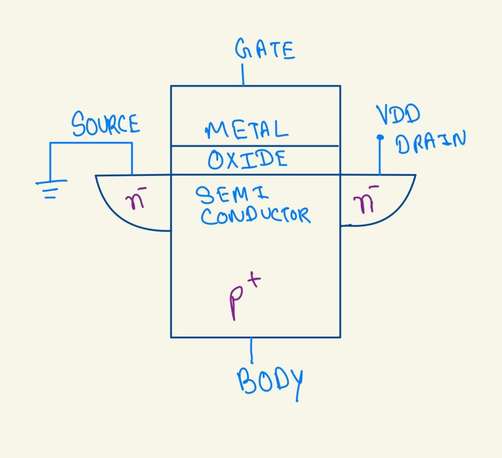
Working:
1. VGS = 0
No inversion channel exists between the source and drain, so ideally no drain current flows (ignoring leakage currents). Electrons and holes still exist in the semiconductor, but they do not form a conducting path.
2. VGS > 0
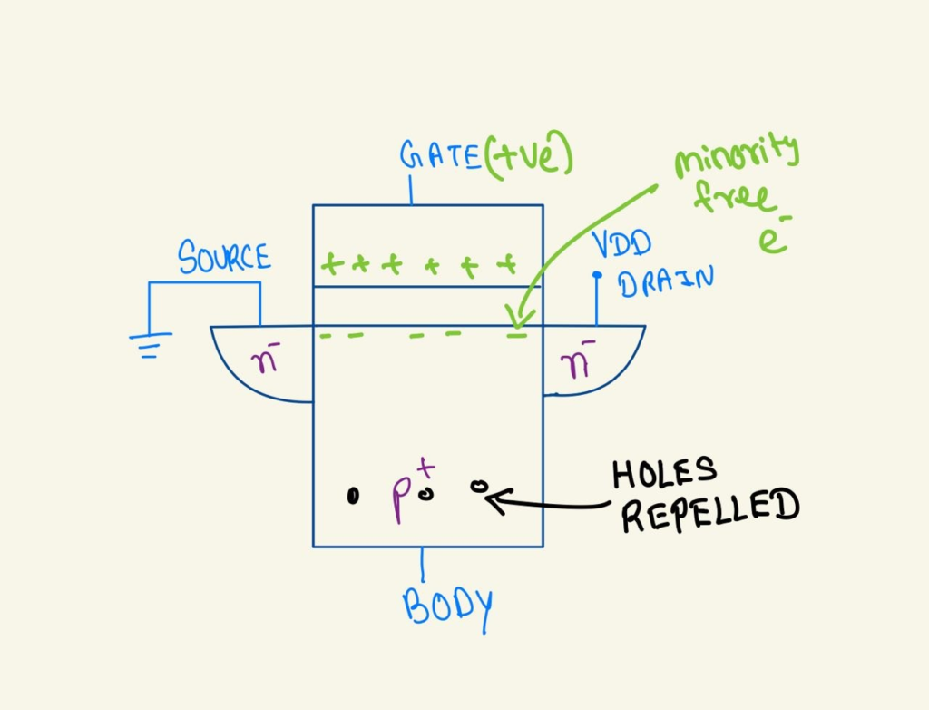
- When a positive voltage is applied to the gate, an electric field is created across the oxide. Since the gate is insulated by the oxide layer, electrons cannot enter the gate. Instead, electrons inside the semiconductor are attracted toward the surface beneath the oxide, while holes are pushed deeper into the substrate.
- As holes move away from the surface, they leave behind fixed negatively charged acceptor ions. This region is called the depletion region because it is depleted of majority carriers (holes), leaving behind fixed negatively charged acceptor ions.
3. VGS > Vth (Threshold Voltage)
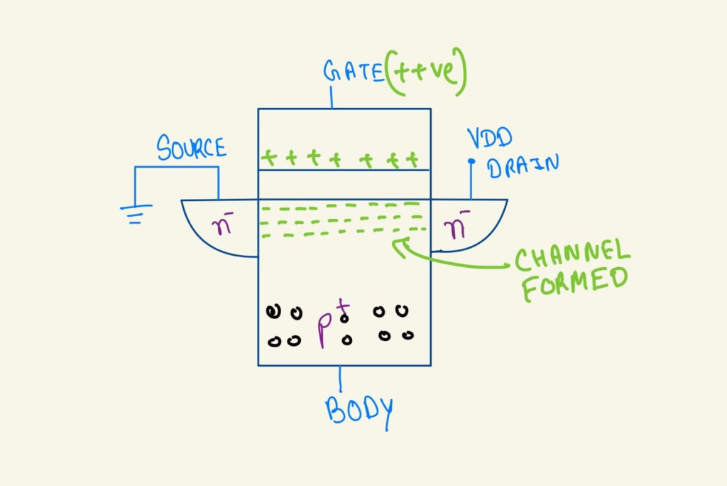
- Once the gate voltage exceeds the threshold voltage (Vth), enough electrons accumulate at the silicon–oxide interface to form an inversion layer. This inversion layer behaves like an n-type channel connecting the source and drain.
- When a drain-to-source voltage (VDS) is applied, electrons drift from the source to the drain, producing a conventional current from the drain to the source.
- This process is called inversion because the surface changes from behaving like p-type silicon to behaving like n-type silicon.
4. VGS < 0
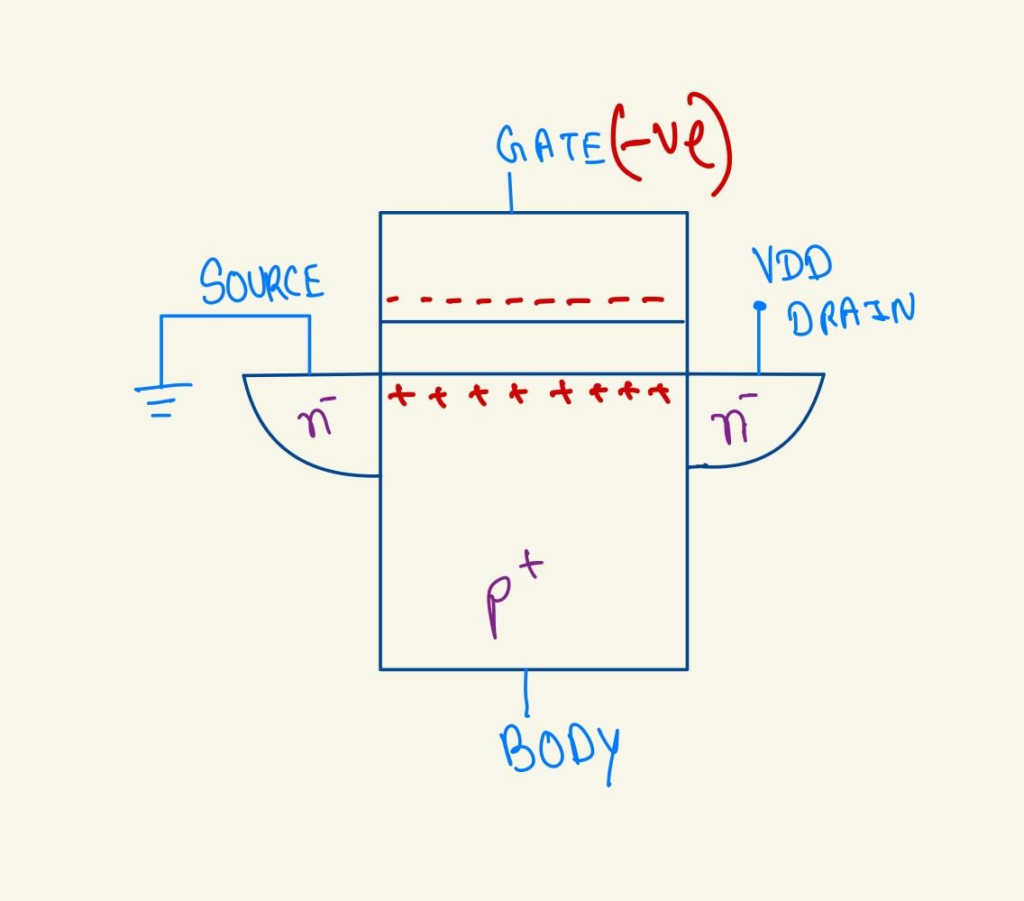
- A negative gate voltage attracts holes toward the surface and pushes electrons away. Since no inversion channel can form, the MOSFET remains OFF.
- This condition is called accumulation because holes accumulate near the silicon surface.
Interview Questions :
- Why is oxide used? What’s the role of oxide? –> The oxide layer electrically insulates the gate from the semiconductor while allowing the electric field to control the channel.
- Why SiO2 (silicon dioxide)? –> Silicon dioxide (SiO₂) is used because it forms an excellent interface with silicon, has high electrical insulation, low defect density, and good thermal stability. These properties improve device reliability and reduce threshold voltage variation.
- Why are MOSFETs used? –> MOSFETs are widely used because they are voltage-controlled devices with extremely high input impedance, low power consumption, fast switching speed, and high integration density. They are ideal for digital ICs and modern VLSI circuits. Also, MOSFETs can drive very high fanout/load. Although MOSFETs can drive multiple gates (high fanout), increasing the load capacitance increases propagation delay.
For Feedback and more updates, join this Telegram channel: https://t.me/thesiliconpath